This analysis opens with the datasheet highlights: a single‑supply, rail‑to‑rail input/output amplifier with a listed gain‑bandwidth product near 10 MHz, designed for low‑power portable designs, and sample pricing starting around $0.92. The purpose is practical and measurement‑focused: summarize the device’s key electrical characteristics, translate the published specs into real‑world expectations, provide a reproducible bench test plan, and offer BOM and layout recommendations for product engineers.
The goal is to help designers decide whether the part fits precision buffer, sensor front‑end, or low‑power analog chains by combining datasheet interpretation, measurement methodology, and procurement guidance in a concise, data‑first format tailored for US engineering teams.
1 — Background: MAX74821 at a glance
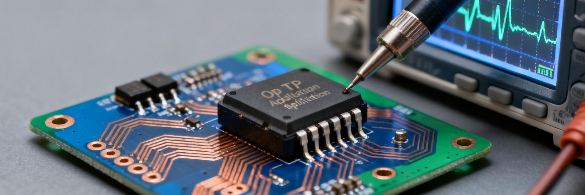
The MAX74821 is positioned as a low‑power rail‑to‑rail op amp suited to battery‑operated and small‑signal systems. Key marketing points emphasize single‑supply operation, modest wideband performance (~10 MHz GBW), and low unit cost at small volumes. This section compresses the most relevant electrical attributes into a quick reference so engineers can compare it against application needs before committing to prototype tests.
Key electrical characteristics to summarize
| Parameter | Symbol | Typical | Min / Max | Units | Test conditions / Notes |
|---|---|---|---|---|---|
| Supply range | VCC | ~1.8–5.5 | check datasheet | V | Single‑supply operation; verify absolute limits and recommended ranges |
| Quiescent current | IQ | tens of μA | see table | μA per amp | Depends on supply; measured per amplifier |
| Input common‑mode range | VIC | Rail‑to‑rail | within rails ± few mV | V | Caveats near rails under certain loads |
| Output swing | Within tens of mV to rails | Depends on RL | V | Specified under RL = 10 kΩ / 2 kΩ in datasheet | |
| Gain‑bandwidth | GBW | ~10 | — | MHz | Typical small‑signal figure; measured in closed loop |
| Slew rate | SR | tens to low hundreds | — | V/μs | Large‑signal transient behavior depends on load |
| Input offset | VOS | μV–mV range | datasheet bounds | mV | Important for sensor front‑ends; drift matters |
| Noise | low‑μV/√Hz | — | nV/√Hz | Input‑referred; check frequency band of interest | |
| CMRR / PSRR | moderate to high | — | dB | Specified at frequency points; critical in single‑supply systems | |
| Output drive | tens mA | see safe dissipation | mA | Depends on supply and thermal limits | |
| Package / pins | small SMD | see ordering codes | Pin count and footprint matter for BOM | ||
| Temperature rating | industrial range | check datasheet | °C | Junction/ambient limits depend on PCB thermal design |
Typical applications and target use-cases
This amplifier suits precision buffer stages for sensors, low‑power data‑acquisition front‑ends, portable instrumentation, and general‑purpose rail‑to‑rail signal chains. Trade‑offs vs. higher‑GBW or lower‑noise amplifiers are straightforward: choose this family when energy per operation and cost are prioritized over extreme bandwidth or the lowest possible noise.
2 — Datasheet deep-dive: what the specs really mean
Analog performance metrics explained (op amp performance)
GBW determines the closed‑loop bandwidth you can expect at a given gain: for example, a 10 MHz GBW gives roughly 1 MHz usable bandwidth in a gain of 10. Slew rate limits how fast large transients can be followed; insufficient SR leads to slew‑limited edges in pulse applications. Input offset and drift map directly to sensor zero‑offset error; input‑referred noise density determines resolution for low‑level signals. Open‑loop gain sets achievable DC accuracy and linearity. These specs together define whether an op amp meets a given signal‑chain target.
Supply, I/O and thermal limits
Supply range and rail‑to‑rail I/O claims must be interpreted with conditions: output swing is typically specified into high‑impedance loads and degrades into heavier loads. Input common‑mode may approach rails but performance (drift, CMRR) often worsens near extremes. Quiescent current scales with supply and temperature, so report IQ under the test conditions. Thermal derating and maximum junction temperature determine allowable continuous output drive and must be translated into PCB thermal budgets.
3 — Benchmarks & test methodology (reproducible, data-driven)
Suggested bench tests and setups
Provide step‑by‑step procedures for GBW (measure closed‑loop gain vs frequency in gains of 1 and 10), small‑signal frequency response, slew‑rate (apply large step and capture dV/dt), large‑signal settling time, THD+N (sine drive at relevant amplitudes), input‑referred noise (spectrum analyzer in low‑noise setup), output drive vs RL, input common‑mode behavior, and PSRR/CMRR. Use standard test fixtures: short feedback traces, bypass caps at the package, RL = 10 kΩ and 2 kΩ, supply rails representative of target application, and oscilloscope bandwidth >5× test frequency.
Include these plots: transfer function (magnitude/phase), FFT/THD, slew waveform, noise spectrum, and output swing vs load. Label axes and include measurement settings (scope bandwidth, averaging, source impedance) for reproducibility.
How to interpret and benchmark results vs. peers
Normalize comparisons on cost, power, and performance: present bandwidth‑per‑mA, noise‑per‑mA, and output‑swing under identical loads. Use delta and percent differences rather than raw value claims to highlight practical gaps. For example, show percent bandwidth loss at RL = 2 kΩ vs RL = 10 kΩ to showcase load sensitivity.
4 — Pricing, procurement & BOM considerations
Pricing structure and volume guidance
Report sample/unit price, and two volume breaks (1k and 10k) with a note on expected lead‑time volatility. Include freight and packaging assumptions for accurate BOM cost. Present a simple price table so readers can estimate per‑unit BOM impact and evaluate cost trade‑offs for multi‑sourcing strategies.
| Quantity | Unit price (approx.) |
|---|---|
| Sample / single | $0.92 |
| 1k pcs | ~$0.60 (estimate) |
| 10k pcs | ~$0.40 (estimate) |
Drop-in alternatives, footprint and supply-risk mitigation
When recommending substitutes, compare electrical equivalence (supply range, GBW, SR, offset, noise) and pin‑compatibility. Mitigation tactics include multi‑sourcing qualified alternatives, designing for alternate footprints, and ensuring layout modularity so an op amp swap requires minimal PCB change. Document acceptance tests for any substitute.
5 — Design checklist & practical recommendations
When to choose the MAX74821 (buyer's checklist)
- Battery or low‑power system requiring single‑supply rail‑to‑rail I/O and modest bandwidth.
- Application tolerance for moderate noise and limited large‑signal slew capacity.
- Cost‑sensitive BOM where sub‑$1 samples and low IQ per channel are priorities.
- Not ideal if the application needs multi‑MHz wideband at high output drive or ultralow noise for precision ADC front‑ends.
PCB layout, decoupling and stability tips
Place bypass capacitors (0.1 μF ceramic + 1 μF polymer) as close to the supply pins as possible, use a star ground or solid plane, and minimize loop area between feedback network and input pins. Add small series resistances or snubbers when driving capacitive loads. Include test points for supply, input, output, and feedback node to simplify characterization and debug.
Summary
In short verdict form: the MAX74821 is a cost‑effective, low‑power rail‑to‑rail amplifier that delivers roughly 10 MHz GBW suitability for sensor buffers and portable analog chains at a sample price near $0.92. Its strengths are single‑supply convenience and low IQ; trade‑offs include limited large‑signal slew and moderate noise compared with premium amplifiers. Run the benchmark suite above to verify behavior in your load and thermal environment.
Suggested long‑tail keywords: "MAX74821 op amp datasheet", "MAX74821 specs and bench tests", "MAX74821 low‑power rail‑to‑rail op amp performance". Meta description (≈150 chars): "MAX74821 op amp specs, bench tests, and pricing: a data‑driven guide to performance vs cost for low‑power rail‑to‑rail designs."
Key summary
- Quick spec snapshot: rail‑to‑rail I/O, single‑supply, ~10 MHz GBW, low μA quiescent current — ideal for portable sensor buffers and general‑purpose analog front‑ends.
- Bench focus: measure GBW, slew, noise spectrum, THD+N, and output swing vs load for apples‑to‑apples comparisons.
- Procurement tip: include sample, 1k and 10k pricing lines on BOM and plan for multi‑sourcing and footprint alternatives.
Frequently Asked Questions
Is the MAX74821 suitable for precision sensor front-ends?
Yes if the sensor requires rail‑to‑rail buffering with low quiescent current and moderate resolution; however, for highest precision or lowest noise, compare input‑referred noise and offset drift against tighter‑spec alternatives and consider post‑amplifier filtering or offset calibration.
What bench tests validate MAX74821 specs?
Essential tests are closed‑loop frequency response (GBW), slew‑rate measurement, large‑signal settling, THD+N via FFT, input‑referred noise spectrum, and output swing under representative RL values. Document test conditions to ensure reproducible comparisons.
How should designers report MAX74821 specs in documentation?
Report measured values alongside datasheet conditions (supply, RL, gain config, temperature). Use normalized metrics (bandwidth‑per‑mA, noise‑per‑mA) and delta plots vs. competitors for clear decision data.
What are the primary procurement considerations for the MAX74821?
Review volume price breaks at 1k and 10k quantities, monitor lead‑time volatility, and plan for multi‑sourcing and footprint alternatives to mitigate supply‑chain risks.




