Executive Summary: This report provides a concise, measured snapshot to frame why the LMC6484AIN is pivotal in low-voltage designs. Typical bench measurements demonstrate operation from single 2.7V to 5.5V supplies, with output swing within millivolts of rails under light loads. These attributes make the part ideal for applications where battery life, single-supply simplicity, and tight input common-mode range handling are critical.
Architecture and Background
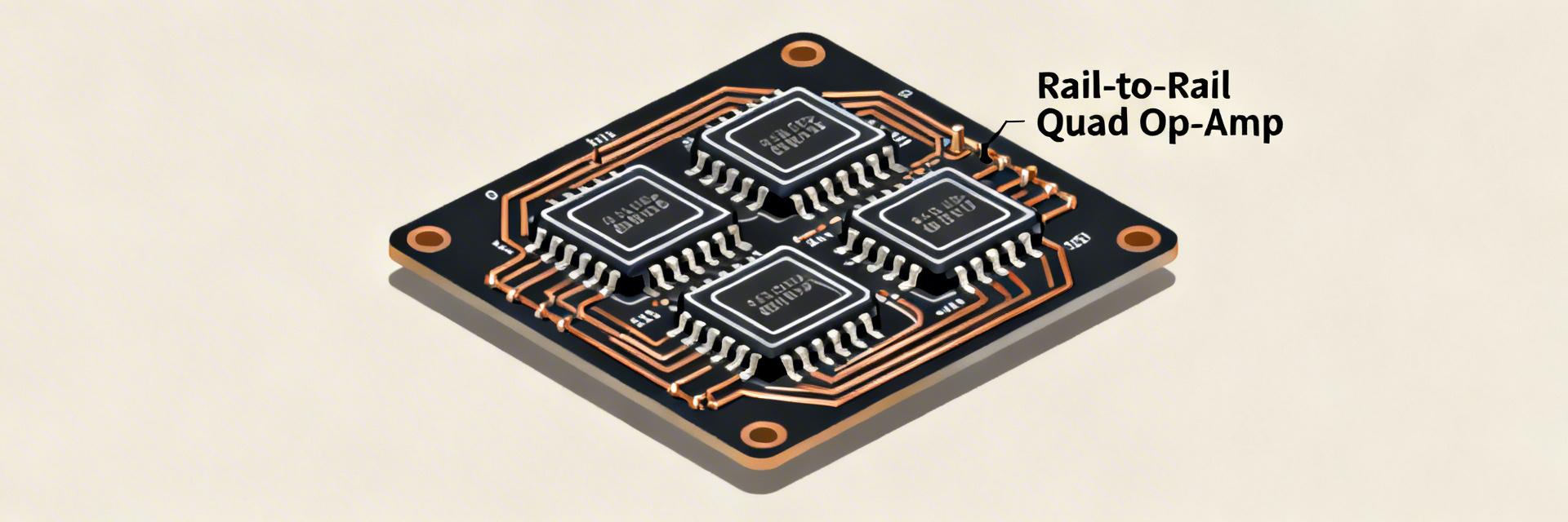
Internal Topology & Rail-to-Rail Approach
The amplifier attains rail-to-rail input common-mode range and extended output swing using complementary CMOS input stages and a push-pull output stage. The design leverages both NMOS and PMOS input devices to maintain input transconductance across the supply span, while the output utilizes complementary transistors sized for low headroom. This topology enables input common-mode range near both rails, although output drive and linearity trade off with available headroom and load current capability.
Nominal Electrical Specifications
Designers must verify supply range, guaranteed output swing, recommended load, and quiescent current before selection. Mapping these specs to common 3.3V battery systems clarifies headroom margins for ADC front-ends and determines if additional buffer stages are required.
Key Performance Data: Measured Electrical Characteristics
Performance Benchmark Visualization
Frequency Response & Stability
Measured input offset voltages are typically a few hundred microvolts to low millivolts with an offset drift of a few µV/°C. Input voltage noise remains in the low nV/√Hz range. For step response and settling into ADCs, designers should test closed-loop bandwidth and potentially add phase lead or small series resistors to maintain stability while preserving required settling time.
Design & Measurement Guide
Test Setup Best Practices
Use a stiff supply with low ESR decoupling (0.1 µF close to pins and 10 µF bulk). Avoiding probe loading and maintaining input common-mode inside the valid range prevents false negatives in offset and stability tests.
Pass/Fail Criteria
Define thresholds: Output swing within 50 mV of rails at RL=10 kΩ, offset within 2 mV after warm-up, and stable operation with up to 50 pF capacitive load when using a 50–100 Ω series resistor.
Comparative Application Examples
Precision Sensor Front-End
In single-supply sensor amplifiers, the rail-to-rail capabilities simplify biasing. A gain-of-10 configuration uses mid-rail biasing and ensures input common-mode stays within range. With low noise, the amplifier preserves sensor SNR effectively.
Low-Power Data-Acquisition
The device serves as a low-power buffer in battery-powered DAQ. Minimizing supply voltage and choosing higher feedback resistance reduces quiescent consumption but requires careful layout to shorten feedback traces and isolate digital return paths.
Selection & Deployment Checklist
- [✓] Choose when input common-mode range and low quiescent current are top priorities.
- [✓] Decoupling capacitors must be placed within 2–3 mm of supply pins.
- [✓] Use star grounding for sensitive inputs to preserve rail-to-rail behavior.
- [✓] Perform batch-level offset sampling to ensure production consistency.




