When evaluating dual JFET input op amps, engineers check a short list of measurements first: input offset and bias, common‑mode range, output swing, gain‑bandwidth and slew rate. This datasheet‑focused overview extracts those checkpoint numbers so designers can translate published limits into margin decisions. The goal is to convert datasheet claims into actionable tolerance budgets and bench tests that reveal whether the device meets system requirements.
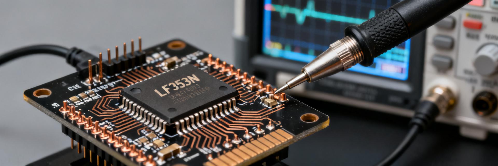
Background: LF353N at a Glance
The LF353N is a low-cost, high-speed, dual JFET input operational amplifier with an internally trimmed input offset voltage. It combines high-voltage JFETs and bipolar transistors on a single monolithic chip.
Package & Pin Functions
Pin assignments determine which nodes need bypassing. Place bypass capacitors close to the V+ (Pin 8) and V− (Pin 4) pins. Keep input traces short and separate analog returns from noisy power grounds. Protecting inputs against ESD and differential overload is critical to prevent junction conduction that violates datasheet conditions.
Datasheet Deep‑Dive: DC & AC Performance
| Parameter | Typical / Design Note |
|---|---|
| Input Offset Voltage | 5 mV (max @ 25°C); requires trim for precision DC |
| Input Bias Current | 50 pA (typical); critical for high-Z integrators |
| Gain‑Bandwidth | 4 MHz; determines loop gain at high frequency |
| Slew Rate | 13 V/µs; limits large-signal audio fidelity |
| Supply Current | 3.6 mA per amplifier; consider thermal dissipation |
Practical DC Tolerances
Offset and bias set the DC error floor. For integrators, low bias is critical as input current integrates to large voltages over time. Actionable: Budget for 10µV/°C drift when operating across industrial temperature ranges.
AC Stability & Speed
The 13 V/µs slew rate is excellent for audio, but ensure slew-induced harmonic content remains below your THD target. Use the rule of thumb f_CL ≈ GBP / Gain to estimate bandwidth flatness. Target closed‑loop gains that keep the operating frequency well below where phase margin drops below 45°.
Layout and Implementation Guidelines
- Decoupling: Use 0.1µF ceramic caps within 2mm of pins + 10µF bulk nearby.
- Capacitive Loads: Add a 10–100Ω series resistor at the output when driving long cables to prevent oscillation.
- High-Z Inputs: Guard sensitive input traces with a grounded copper ring to mitigate leakage currents.
Frequently Asked Questions
How should I budget offset and input bias from the LF353N for a precision DC amplifier?
Budget offset as the sum of worst‑case input offset voltage and the voltage produced by input bias current through source resistance. Measure typical bias on your board and add the datasheet maximum drift over your temperature range. If the combined error exceeds acceptable limits, use trimming or a chopper amplifier alternative.
What headroom margin should I leave from the rails to avoid output clipping?
Leave at least one to two volts of margin from each rail for linear output swing under moderate loads; increase margin if driving heavy loads or using single‑supply operation. Verify on the bench by sweeping output amplitude and monitoring distortion and clipping thresholds.
Which bench tests quickly reveal stability problems claimed by the datasheet?
Run a closed‑loop frequency sweep to compare measured gain and phase against expectations, perform a step test to reveal slew‑limited settling, and inject a capacitive load to check for peaking or oscillation. Document results and compare against datasheet tolerances to decide on compensation or substitution.
When is it necessary to substitute the LF353N with an alternative op-amp?
Substitute when system requirements exceed LF353N limits, specifically for rail-to-rail I/O needs, lower noise floors (<16nV/√Hz), higher slew rates for fast transients, or femto-amp level bias current for ultra-high impedance sensors.




