Introduction
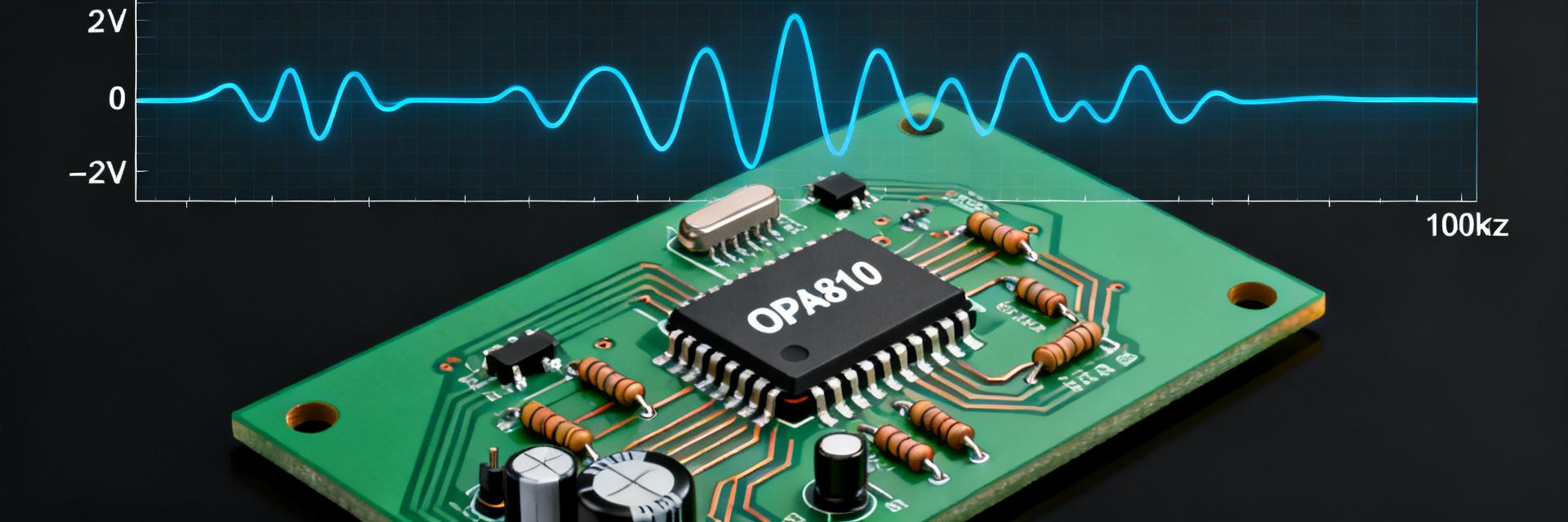
The OPA810QDBVRQ1 appears in many high‑speed precision designs because of a compelling spec set: ≈140 MHz small‑signal bandwidth, roughly 200 V/µs slew rate, wide supply range, and sub‑microvolt typical offset. This article unpacks the official datasheet to clarify which numbers matter in practice, how to validate them on the bench, and how to apply results to sensor front‑ends and buffer stages.
Goal: translate datasheet numbers into actionable design guidance including a focused electrical spec deep‑dive, prioritized performance metrics, a practical test checklist, and simulation/layout tips. The first section summarizes device context and an at‑a‑glance spec list so readers can quickly assess suitability for high‑speed, precision applications.
Device overview & high-level spec snapshot
What the OPA810QDBVRQ1 is and where it fits
Point: This amplifier targets high‑bandwidth, low‑offset applications such as high‑speed buffers and precision sensor front‑ends. Evidence: the part combines rail‑to‑rail I/O behavior with FET‑input characteristics documented in the official datasheet. Explanation: designers will pick it where wide operating voltage, low bias currents, and fast settling are required, especially in systems needing extended temperature support.
Quick reference table
Point: A compact comparison of typical versus maximum values helps prioritize tests. Evidence: the most impactful numbers are supply range, small‑signal bandwidth, slew rate, input bias, and offset. Explanation: use the table and a simple operating‑point note (VCC, RL, Ta) to set up initial validation and variance expectations.
| Parameter | Typical | Maximum / Test Conditions |
|---|---|---|
| Supply range | ±2.5 V to ±12 V | Specified in datasheet, varies with rail |
| Small‑signal bandwidth | ~140 MHz (closed‑loop) | Depends on gain and supply |
| Slew rate | ~200 V/µs | Measured with specified load |
| Input bias current | pA range typical | Increases with temperature |
| Offset | sub‑µV typical | Max per datasheet under conditions |
Electrical characteristics deep dive
Frequency response, GBW and small‑signal bandwidth
Point: GBW and small‑signal bandwidth determine closed‑loop gain response and phase margin. Evidence: the datasheet provides open‑loop gain versus frequency and closed‑loop response curves. Explanation: recreate open‑loop gain vs frequency and closed‑loop bode plots in simulation to predict peaking and bandwidth tradeoffs at intended gains and supply voltages.
Slew rate, large‑signal behavior, and distortion
Point: Slew rate dictates large‑signal settling and distortion at high amplitudes. Evidence: datasheet slew and large‑signal tests set expectations for THD and IMD under defined loads. Explanation: define pass/fail thresholds (for example, clean 10 MHz sine at target amplitude) and test with step responses and two‑tone IMD to confirm usable large‑signal bandwidth.
Precision & bias parameters: offset, noise, inputs
Input offset, bias current, and drift
Point: Offset and bias set the floor for DC accuracy and long‑term stability. Evidence: typical versus max offset and pA‑scale bias current are tabulated in the datasheet with temperature coefficients. Explanation: use averaging, zeroing procedures, and calibration to manage drift; when bias matters, guard traces and input filtering reduce error during measurement and operation.
Noise performance and its system impact
Point: Noise density and integrated RMS noise determine detectability of low‑level signals. Evidence: the datasheet noise plots show frequency‑dependent voltage and current noise. Explanation: integrate noise density across the intended bandwidth to estimate RMS noise; then compare to signal amplitude to set required gain and filtering for target SNR.
Thermal, reliability, and operating limits
Temperature range, power dissipation, and derating
Point: Thermal limits constrain safe continuous operation and affect noise/offset. Evidence: thermal resistance and junction‑vs‑ambient specs are provided in the official datasheet. Explanation: calculate power dissipation from supply and quiescent current, apply θJA to estimate junction temperature, and follow PCB thermal practices (copper pours, thermal vias, decoupling placement) to remain within derated limits.
Reliability‑related specs and margins
Point: Extended qualification and stress testing indicate suitability for harsh environments. Evidence: temperature range and stress parameters in the part documentation guide margining. Explanation: apply conservative margins for automotive or safety‑critical designs—reduce allowable power, tighten thermal budget, and verify performance at elevated temperatures during validation.
Validation, simulation, and practical design checklist
Bench validation checklist (how to test the key specs)
Point: A focused bench checklist speeds verification of the most relevant Key Specs. Evidence: recreate datasheet test conditions (Vcc, RL, probe loading) and use calibrated instruments. Explanation: include required instruments, probe grounding, test steps for bandwidth, slew, offset, bias, and noise, and define pass/fail tolerances tied to application‑level requirements.
Simulation and layout tips for reliable performance
Point: Simulation and layout prevent surprises and preserve bandwidth. Evidence: SPICE models and parameter tables in the datasheet allow predictive AC, transient, and noise simulations. Explanation: verify models with AC and transient runs, place local decoupling close to supply pins, keep input traces short and guarded, and maintain solid ground returns to minimize parasitic inductance and maintain stability.
Summary
Critical takeaways: prioritize small‑signal bandwidth and slew for high‑frequency fidelity, attend to offset and low bias for precision sensing, and validate thermal margins early. The OPA810QDBVRQ1 offers a balanced mix of speed and precision but requires careful layout and measurement to realize datasheet performance; follow the bench checklist and SPICE verification before prototyping.
Key Summary
- The OPA810QDBVRQ1 combines ~140 MHz bandwidth and ~200 V/µs slew rate, making it suitable for high‑speed buffers and sensor front‑ends when designed with correct loading and supply margins.
- Measure offset and bias with guarded setups and averaging; convert noise density to RMS over the application bandwidth to set gain and filtering requirements for target SNR.
- Thermal and PCB practices directly affect measurable performance—calculate dissipation with θJA, derate for ambient, and enforce tight decoupling and short input returns for stability.




