The INA299A2IDBVR combines a wide common‑mode input window (negative to high voltages), single‑supply operation, low quiescent current, and selectable gains to address high‑side and bidirectional current sensing. This datasheet‑focused snapshot highlights why those numbers matter: they permit direct sensing on rails that sit well above logic rails, reduce power draw in distributed monitoring, and let designers trade span for resolution with simple gain selection. Use these figures to rapidly assess fit for battery supervision, server power rails, and motor‑drive telemetry.
Key numbers to note up front: common‑mode range spanning negative voltages up to high system rails, supply from a single 3.3–5.5V source (device dependent), quiescent current in the low microamp to single‑digit milliamp region, and fixed gain variants for 50–500mV shunt spans. Those figures define where the INA299A2IDBVR best fits in a system and which design cautions to apply.
1 — Product overview and intended uses (background)
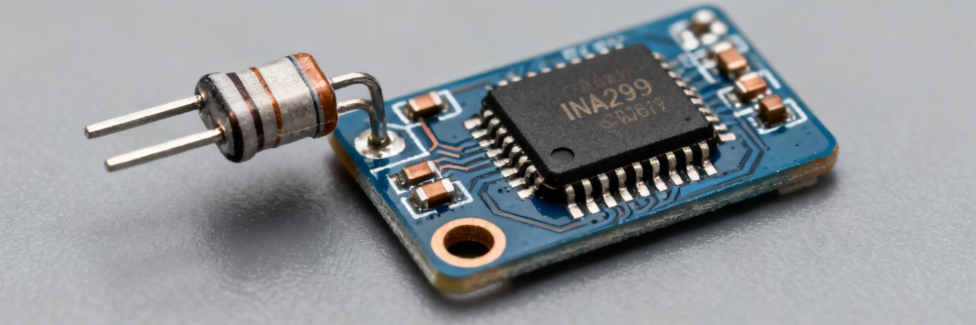
What the INA299A2IDBVR is and where it fits
The INA299A2IDBVR is a current‑sense front end optimized for high‑side and bidirectional measurements: a precision amplifier that converts small shunt voltages into rail‑referenced outputs. Typical domains include power‑rail monitoring for servers, battery management, motor controllers, and distributed power systems where sensing must tolerate elevated or negative common‑mode voltages. Designers pick this family when they need integrated gains and low quiescent current for multi‑channel or always‑on monitoring.
Package, pinout and ordering info (what to check on the datasheet)
When reading the package drawing check pin functions (IN+, IN−, VOUT, VCC, GND) and thermal pad recommendations; thermal pad soldering and exposed pad area directly affect dissipation. For ordering, confirm the gain variant code and package suffix — variants provide discrete gains or fixed full‑scale shunt spans. Verify the “key specs” block in the datasheet to confirm the gain choices match your maximum shunt voltage and ADC input range needs.
2 — Operating ranges & absolute maximums (data analysis)
Supply voltage, common‑mode range and input limits
Typical recommended supply: single‑supply operation around 3.3–5.5V; device supports sensing with the inputs at negative voltages up to tens of volts above ground (refer to device table for exact limits). The common‑mode window allows direct high‑side sensing without external level shifting. Absolute maximums exceed recommended ranges; do not operate into absolute maxima continuously — treat them as survivability limits and add margin for transients and manufacturing variation.
Thermal and power dissipation limits
Check maximum ambient and junction temperatures and the package thermal resistance (θJA). Higher common‑mode voltages can increase power dissipation through input protection networks and any internal linear elements; derate allowable power with ambient temperature and account for PCB copper and thermal vias. Practical design: keep exposed pad soldered, add copper pour for heat spreading, and force a de‑rating curve of supply and ambient to guarantee safe junction temperatures under worst‑case dissipation.
3 — Electrical performance: gains, bandwidth, noise, accuracy (data analysis)
Gain options, offset, and gain error
Fixed gain variants map to specific full‑scale shunt voltages (for example 50, 100, 250mV spans depending on variant). Higher gain increases resolution but makes offset and offset drift proportionally more significant for low‑current measurement. Input offset and offset drift set the measurement floor: when measuring microamp‑level currents through milliohm shunts, offset plus gain error can dominate accuracy — compute worst‑case error by summing offset×gain and percent gain error relative to your expected shunt voltage.
Bandwidth, slew, CMRR, PSRR, and noise
Bandwidth (hundreds of kHz typical) restricts pulse and transient fidelity — use faster parts or external filtering for very short current pulses. CMRR and PSRR values indicate how well common‑mode swings and supply noise are rejected; high CMRR is critical in noisy power environments. Expect trade‑offs: selecting higher gain improves sensitivity but amplifies noise and offset; add low‑pass filtering or oversample ADCs to recover SNR for steady measurements.
4 — Typical application circuits & measurement methods (methods/guide)
Unidirectional vs. bidirectional sensing circuits
For unidirectional sensing place the shunt on the high side with the amplifier configured to read positive shunt voltages only; for bidirectional use a mid‑scale reference or a variant that supports bipolar outputs and center the ADC reference so positive/negative currents map above/below midpoint. Keep sense traces short and, for high‑side shunts, ensure the amplifier common‑mode rating covers the rail voltage plus expected transients.
Output conditioning and ADC interface
Map amplifier output to ADC input range by selecting the right gain variant or using a small level‑shift network. Add series resistors and clamping diodes to protect ADC inputs, and use a small RC on the output (low value resistor, 10–100Ω, and 10–100nF cap) to filter noise without adding instability. Verify ADC LSB mapping by calculating volts per amp: (shunt mV×gain)/LSB to ensure adequate resolution across the measurement range.
5 — PCB layout, protection, and reliability tips (methods / case)
Layout and grounding best practices
Use short sense traces and Kelvin routing from the shunt to the amplifier IN+ and IN− pins. Place input filter components close to the device, keep ground returns low impedance, and use a star ground if mixed power domains exist. Route the thermal pad to a large copper pour with multiple vias to the internal layers to lower θJA and maintain stable temperature during long measurements.
Overvoltage and ESD protection strategies
Protect against transients with series resistors, TVS diodes sized for expected common‑mode excursions, and input clamps to device rails. For repetitive pulses, perform pulse‑overstress testing and include margin beyond the datasheet absolute maximums. Include ESD test points and design verification tests that cycle junction temperature and apply controlled overvoltage pulses to validate protection strategy.
6 — Limits, common failure modes, and troubleshooting checklist (action)
Common pitfalls when using the INA299A2IDBVR
Typical failures come from exceeding common‑mode or input limits, saturating the amplifier by picking a gain that yields outputs outside the ADC range, poor decoupling, and long sense traces that pick up noise. Misreading ordering codes can lead to wrong gain variants, so confirm the part marking and datasheet ordering table before PCB assembly.
Quick troubleshooting & verification steps
Stepwise checks: confirm VCC and ground; measure IN+ and IN− common‑mode against allowed window; apply a known current through the shunt and verify output proportionality; inspect layout for long or looped sense traces. Use an oscilloscope to check transient response and verify that the output doesn’t rail under expected shunt voltages. Establish pass/fail criteria for production based on offset and gain error limits.
| Key spec | Typical value / guidance |
|---|---|
| Supply | Single 3.3–5.5 V (device dependent) |
| Common‑mode | Negative to high‑rail sensing (see datasheet absolute limits) |
| Gains | Fixed variants for various full‑scale shunt mV spans |
| Quiescent current | Low μA–mA class (optimized for always‑on) |
| Bandwidth | Hundreds of kHz (affects pulse fidelity) |
| Thermal | θJA dependent on soldering and PCB copper; de‑rate with ambient |
Summary
The INA299A2IDBVR offers a compelling mix of wide common‑mode tolerance, selectable gain, and low quiescent current that makes it well suited for high‑side and bidirectional current measurement in battery systems, server rails, and motor controllers. Respect the datasheet operating ranges and thermal limits, choose the correct gain variant for your shunt, and follow PCB layout and protection guidance to achieve the specified accuracy and reliability.
- The INA299A2IDBVR enables direct high‑side sensing across negative and elevated rails; confirm common‑mode limits versus your system transients.
- Select the gain variant to match shunt full‑scale voltage so offset and noise don’t dominate low‑current accuracy.
- PCB thermal pad soldering and copper pours are required to meet thermal limits; derate at higher ambient temperatures.
FAQ
What common‑mode voltages can the INA299A2IDBVR tolerate for high‑side sensing?
Refer to the datasheet common‑mode table for exact numbers, but the device is designed to tolerate negative inputs up to ground and positive inputs up to high system rails used in power distribution. Treat absolute maximums as survival limits and size protection for transients; include margin for hot‑plug and switching spikes.
How do I choose the right gain variant for my shunt and ADC?
Pick the variant whose full‑scale shunt voltage times gain fits within your ADC input range with headroom for offset and transients. Calculate volts per amp = (shunt resistance × gain) and then LSBs per amp = (volts per amp)/ADC LSB. Ensure offset×gain doesn’t consume unacceptable dynamic range at the low end.
How should I test my PCB design to verify reliability with the INA299A2IDBVR?
Include pulse‑overstress with expected current spikes, thermal cycling to validate solder joints and thermal dissipation, and ESD testing on input pins. Validate production units against offset and gain acceptance criteria using a calibrated current source through the shunt and record output deviation over temperature.
What are the common failure modes of the INA299A2IDBVR and how can they be prevented?
Common failures stem from exceeding absolute maximum common-mode input limits, amplifier saturation due to mismatched gain settings, and long sense traces picking up system noise. These are prevented by keeping Kelvin connections short, adding input decoupling capacitors, and ensuring proper thermal routing through a dedicated PCB copper plane.




